一. Information provided by the hardware
1. Accurate schematic diagrams include written documents and electronic files, as well as correct network lists;
2. Formal BOM with component code. For components that are not in the package library, the hardware engineer should provide the DATASHEET or the real object, and specify the definition order of the pins;
3. Provide the general layout of the PCB or the placement of important units and core circuits. Provide the PCB structure diagram, which should indicate the PCB shape, mounting holes, positioning components, forbidden areas and other relevant information;
二. Basic design requirements
1. High current components and networks above 1A;
2. Important clock signals, differential signals and high-speed digital signals;
3. Simulate small signals and other easily interfered signals;
4. Other signals with special requirements;
三. Special requirements
1. Differential wiring, shielded network, characteristic impedance network, equal delay network, etc.;
2. Prohibited wiring area of special components, tin offset, solder mask window opening and other special requirements for structures;
3. Carefully read the schematic diagram, understand the circuit architecture, and understand the working conditions of the circuit;
4. On the basis of full communication with hardware engineers, confirm the key network in PCB and understand the design requirements of high-speed components;
四, the packaging of fixed components
1. Open the netlist and browse through all the packages to ensure that the packages of all components are correct and the package of all components is included in the component library. All the information in the netlist is in capital letters, and there is a problem with loading one side, or the PCBBOM is not continuous, and the components The specific naming is uniformly named according to the company's specifications;
2. All standard components are packaged in the company's unified component library;
3. For packages that do not exist in the component library, the hardware engineer should provide the component DATASHEET or the actual object to build the library by a special person and ask the other party to confirm;
五. Establish PCB board frame
1. Create PCB files according to the PCB structure diagram or corresponding templates, including installation holes, forbidden areas and other related information;
2. Dimensions. The precise structure of the PCB should be marked in the drilling layer, and closed dimensions cannot be formed;
六. Import the network table
1. Import the netlist and eliminate all loading problems. Each EDA software is different, and how to deal with it can be found in relevant tutorials;
2. If EDA software is used, the netlist must be imported more than twice (without any prompt information) to confirm that the import is correct;
七. PCB layout
1. First, determine the reference point. The general reference point is set at the intersection of the left and bottom border lines (or the intersection of extension lines) or the first pad of the plug-in of the printed board;
2. Once the reference point is determined, component layout and wiring shall be based on this reference point. 10-25MIL grid is recommended for layout;
3. Fix and lock all the components with positioning requirements according to the requirements;
4. Basic principles of layout:
①Follow the principle of first difficult and then easy, first big and then small;
② The layout can refer to the schematic diagram and rough layout provided by the hardware engineer, and place the main original devices according to the law of signal flow;
③The overall connection should be as short as possible, and the key signal line should be the shortest;
④ strong signal, weak signal, high voltage signal and weak voltage signal should be completely separated;
⑤ The interval between high-frequency components should be sufficient;
⑥ Separate analog signal and digital signal;
5. The circuit parts with the same structure should adopt a symmetrical layout as much as possible;
6. Optimize the layout according to the standards of uniform distribution, balanced center of gravity, and beautiful layout;
7. Components of the same type should be consistent in the X or Y direction. The same type of polarized discrete components should also strive to be consistent in the X or Y direction, so as to facilitate production and debugging;
8. The placement of components should be convenient for debugging and maintenance. Small components cannot be placed next to large components, and there should be enough space around the components that need to be debugged. The heating element should have enough space to facilitate heat dissipation. Thermal components should be kept away from heating components;
9. The distance between DIP components should be greater than 2mm. The distance between BGA and adjacent components is greater than 5mm. The distance between small chip components such as resistors and capacitors is greater than 0.7mm. The outer side of the patch component pad and the outer side of the adjacent plug-in component pad should be greater than 2mm. The 5 mm around the crimping components cannot place plug-in original devices. Mounting components cannot be placed within 5mm around the soldering surface;
10. The decoupling capacitor of the integrated circuit should be as close as possible to the power supply pin of the chip, and the principle is the closest to the high frequency. Make the shortest loop between it and the power supply and ground;
11. Bypass capacitors should be evenly distributed around the integrated circuit;
12. When laying out components, components using the same power supply should be considered to be placed together as much as possible to facilitate future power distribution;
13. The placement of resistive devices for impedance matching purposes should be reasonably arranged according to their properties;
The layout of matching capacitors and resistors should be clearly defined. For multi-load terminal matching, it must be placed at the farthest end of the signal for matching; ②The layout of the matching resistors should be close to the driving end of the signal, and the distance generally does not exceed 500MIL;
14. Adjust characters. All characters cannot be uploaded to the disk, and it is necessary to ensure that the character information can be clearly seen after assembly. All characters should be consistent in X or Y direction. The size of characters and silk screen should be uniform;
15. Place the MARK point of the PCB;
八. PCB wiring
1. Wiring priority
①Principle of density and looseness: start wiring from the devices with simple connection relationship on the printed board, and start wiring from the area with the loosest connection to adjust the personal state;
② Core priority principle: For example, core parts such as DDRRAM should be wired first, and similar signal transmission lines should provide dedicated layers, power supplies, and ground loops; other secondary signals should be considered as a whole and cannot conflict with key signals;
③ Key signal lines are prioritized: key signals such as power supply, analo small signal, high-speed signal, clock signal, and synchronization signal are prioritized for wiring; 2. Ground loop rules:
The minimum rule of the loop is that the area of the loop formed by the signal line and its loop should be as small as possible, and the loop area should be as small as possible. The smaller the loop area, the less external radiation and the smaller the interference from the outside world. In response to this rule, when dividing the ground plane, the distribution of the ground plane and important signal traces should be considered to prevent problems caused by slotting in the ground plane of the mountain; in the double-layer board design, leave enough space for the power supply. In the case of space, the remaining part should be filled with the reference ground, and some necessary vias should be added to effectively connect the double-sided signals. For some key signals, ground wire isolation should be used as much as possible. For some designs with higher frequencies, Special consideration should be given to the signal loop of the ground plane, and it is recommended to use a multi-layer board;
3. Tamper control:
The mutual interference caused by long parallel wiring between different networks on the PCB is mainly due to the distributed capacitance and distributed inductance between parallel lines. The main measure to overcome crosstalk is to increase the spacing of parallel wiring and follow the 3W rule;
4. Shielding protection:
Corresponding to the ground loop rules, in fact, it is also to minimize the loop area of the signal, and it is mostly used for some important signals, such as clock signals and synchronization signals: for some particularly important and high-frequency signals, copper-axis cables should be considered Shielding structure design, that is, to isolate the distributed lines with ground wires, and also consider how to effectively combine the shielding ground with the actual ground plane;
5. Routing direction control rules:
The wiring direction of adjacent layers is in an orthogonal structure, avoiding different signal lines in the same direction on adjacent layers, so as to reduce unnecessary crosstalk between layers; when it is difficult to avoid this situation due to the limitation of the board structure, especially the signal When the rate is high, it should be considered to use the ground plane to isolate each wiring layer, and use the ground signal line to isolate each signal line;
6. Impedance matching rules;
The wiring width of the same network should be consistent. The change of line width will cause uneven line characteristic impedance. When the transmission speed is high, reflection will occur. This situation should be avoided as much as possible in the design. Under certain conditions, such as connector lead-out wires and similar structures of BGA package lead-out wires, it may not be possible to avoid changes in line width, and the effective length of the inconsistent part in the middle should be minimized;
7. Trace length control rules:
The line length control rule is the short line rule. In the design, the line length should be kept as short as possible to reduce the interference caused by the line length. Especially for some important signal lines, such as clock lines, the oscillator must be placed away from the close to the device. For the case of driving multiple devices, the network topology should be determined according to the specific situation;
8. Chamfering rules:
Acute angles and right angles should be avoided in PCB design, resulting in unnecessary radiation and poor process performance. All line-to-line angles should be ≥135°;
9. Integrity rules for power and ground layers:
For areas with dense via holes, care should be taken to prevent the holes from being connected to each other in the hollowed-out area of the power supply and the formation, forming a division of the plane layer, thereby destroying the integrity of the plane layer, and thus increasing the loop area of the signal line in the formation ;
10. 3W rules:
In order to reduce inter-line crosstalk, the line spacing should be large enough. When the line center distance is not less than 3 times the line width, 70% of the electric field can be kept without interfering with each other, which is called the 3W rule. If you want to achieve 98% of the electric field does not interfere with each other, you can use the 10W rule;
11. 20H rules:
Since the electric field between the power plane and the ground plane changes, electromagnetic interference will be radiated outward at the edge of the board. called the edge effect. The power plane can be retracted so that the electric field is only conducted within the confines of the ground plane. Taking one H (the thickness of the medium between the power supply and the ground) as a unit, if the shrinkage is 20H, 70% of the electric field can be confined within the ground edge; if the shrinkage is 100H, 98% of the electric field can be confined;
九.arrange the stacking order
1. In high-speed digital circuits, the power supply and the ground plane should be as close together as possible, and no wiring is arranged in the middle. All wiring layers should be as close to one plane as possible, and the ground plane is preferred as the isolation layer;
2. In order to reduce the interference between signals, the signal directions of adjacent wiring layers should be perpendicular to each other. If the same direction cannot be avoided, the overlap of signals in the same direction on adjacent signal layers should be avoided as much as possible;
3. Several impedance layers can be set according to the requirements. The impedance layers should be clearly marked as required. Pay attention to the selection of the reference layer, and arrange all signals with impedance requirements on the impedance layer;
十. Set the line width. line spacing
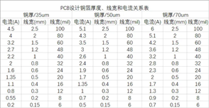
1. When the average current of the signal is relatively large, the relationship between the line width and the current needs to be considered. For the specific situation, please refer to the following table, the current-carrying meter of copper platinum with different thickness and width:
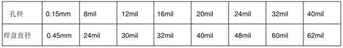
2. The setting of via pad and aperture can refer to the following table: