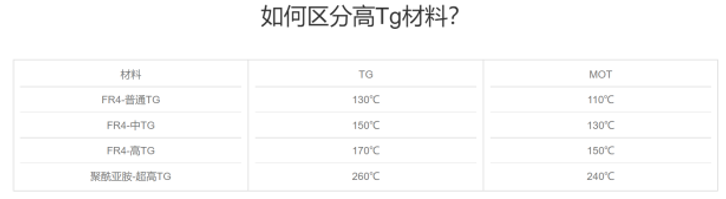
FR-4 is glass fiber epoxy resin copper-clad laminate, a substrate in circuit boards, which can be divided into general FR4 board and high TGFR4 board. Tg is the glass transition temperature, that is, the melting point. The circuit board must be flame-resistant, it cannot burn at a certain temperature, it can only soften. The temperature point at this time is called the glass transition temperature (Tg point), and this value is related to the dimensional stability of the PCB board.

Generally, the Tg of the plate is above 130 degrees, the high Tg is generally greater than 170 degrees, and the medium Tg is greater than 150 degrees. Generally, PCB printed boards with Tg ≥ 170°C are called high Tg printed boards. The Tg of the substrate is increased, and the heat resistance, moisture resistance, chemical resistance, and stability of the printed board will be improved and improved. The higher the TG value, the better the temperature resistance of the board, especially in the lead-free process, there are more high Tg applications.
impedance matching
Impedance matching is mainly used on transmission lines to achieve the purpose that all high-frequency microwave signals can be transmitted to the load point, and almost no signal is reflected back to the source point, thereby improving energy efficiency.
The internal resistance of the signal source is equal to and in phase with the characteristic impedance of the connected transmission line, or the characteristic impedance of the transmission line is equal in magnitude and in phase with the connected load impedance, respectively called the input or output of the transmission line in impedance matching state, referred to as Impedance matching.
Common impedance control values in PCBs are: 100 ohm differential impedance, 90 ohm differential impedance and single-ended 50 ohm impedance. surface treatment
PCB board surface treatment is generally divided into several types. In order to better understand the various problems of your own PCB design, here is a brief introduction:
1) HASL, HASL is the most common surface treatment process in the circuit board industry. It has good solderability and can be used for most electronic products. For other surface treatments, HASL has the advantages of low cost and good solderability; its disadvantage is that the surface is not smooth with immersion gold, especially when large-area windows are opened, tin unevenness is more likely to occur.
2) Immersion tin, the difference between immersion tin and HASL is that it has good flatness, but the disadvantage is that it is extremely easy to oxidize and blacken.
3) Immersion gold, as long as it is "sinking", its flatness is better than that of "spraying". Immersion gold is lead-free. Immersion gold is generally used for gold fingers and key boards. Because gold has low resistance, gold must be used for contact, such as the key board lights of mobile phones. Immersion gold is soft gold. For those that are often plugged and unplugged, gold plating is used. Immersion gold is mainly immersion nickel gold.
4) Gold plating, gold plating has been mentioned in immersion gold, and gold plating has a fatal shortcoming that its weldability is poor, but its hardness is better than immersion gold. This process is generally not used in the design of MID and VR.
Assistant Tip: If there is a requirement for flatness, such as impedance circuit boards (such as microstrip lines) that require frequency, try to use immersion gold technology; generally MID boards with BGA use immersion gold technology.
5) OSP, which mainly relies on the reaction between the potion and the soldered copper skin to produce solderability, the only advantage is fast production and low cost; but because of its poor solderability and easy oxidation, it is generally used less in the circuit board industry.
Core board (Core) fPP sheet (prepreg)
The reinforcing material is impregnated with resin, one or both sides are covered with copper foil, and a plate-shaped material is formed by hot pressing, which is called copper-clad laminate. It is the basic material for PCB, often called substrate. When it is used in the production of multi-layer boards, it is also called core board (CORE).
A sheet-like bonding material synthesized by resin and carrier is called PP sheet. Cores and prepregs are common materials used to make laminated multilayer boards. differential line
The differential signal is that the driver end sends two signals of equal value and opposite phase, and the receiving end judges the logic state "O" or "1" by comparing the difference between the two voltages. The pair of traces that carry differential signals is called a differential trace.
Differential signals, some of which are also called differential signals, use two identical, opposite-polarity signals to transmit one channel of data, and rely on the level difference of the two signals for judgment. In order to ensure that the two signals are completely consistent, they must be kept in parallel during wiring, and the line width and line spacing remain unchanged.
Signal integrity
Signal integrity refers to the quality of the signal on the transmission line. A signal with good signal integrity means that it has the necessary voltage levels to reach when needed. Poor signal integrity is not caused by a single factor, but by a combination of factors in the board-level design. Major signal integrity issues include reflections, oscillations, ground bounce, crosstalk, and more.
signal reflection
A reflection is an echo on a transmission line. A portion of the signal power (voltage and current) is transmitted to the line and reaches the load, but a portion is reflected. If the source and load have the same impedance, the reflection will not occur. Source and load impedance The mismatch will cause reflection on the line, and the load will reflect a part of the voltage back to the source. If the load impedance is less than the source impedance, the reflected voltage is negative; convers, if the load impedance is greater than the source impedance, the reflected voltage is positive. The geometry of the wiring, incorrect Variations in wire termination, transmission through connectors, and discontinuities in power planes can cause such reflections.
Reflection will cause signal overshoot overshoot, undershoot undershoot, ringing, and edge delay, which is a ladder voltage wave.
Crosstalk
Crosstalk is the coupling between two signal lines, and the mutual inductance and mutual capacitance between the signal lines cause noise on the line. Capacitive coupling induces a coupled current while inductive coupling induces a coupled voltage. The parameters of the PCB board layer, the spacing of the signal lines, the electrical characteristics of the driving end and the receiving end, and the line termination method all have a certain influence on the crosstalk.
Inner Layer
The inner electrical layer is a negative layer of the PCB, and its main function is to be used as a power or ground layer, and the power supply is divided when necessary.
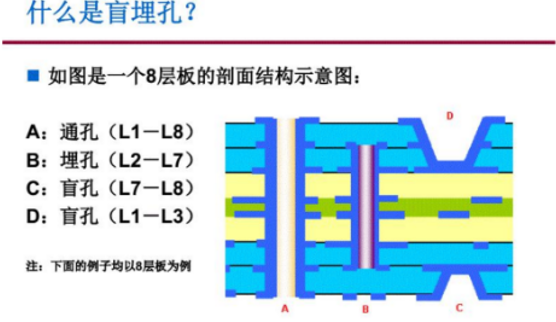
1) Blind hole: A via extending from the middle layer to one surface layer of the PCB. Common ones are first-order and second-order. For example, first-order blind holes refer to the vias from the second layer to the TOP layer or the vias from the penultimate layer to the Bottom.
2) Buried hole: The via hole from one middle to another middle will not extend to the surface layer of the PCB.
Test point:
Generally refers to independent PTH holes, SMT PAD, golden fingers, Bonding fingers, IC fingers, BGA soldering points, and test points that customers test after plug-in. Mark point
The Mark point is the position identification point where the PCB is applied to the automatic placement machine in the circuit board design, also known as the optical point. The selection of Mark points directly affects the placement efficiency of the automatic placement machine. Generally, the selection of Mark points is related to the model of the automatic placement machine. Mark points are generally designed as @1 mm (40 mil) circular graphics. Considering the contrast between the material color and the environment, leave a non-soldering area 0.5 mm (19.7 mil) larger than the optical positioning reference symbol, and no characters are allowed, as shown in the figure below.
The optical positioning fiducial symbols on the same board should be the same as the background of the adjacent inner layer, that is, the presence or absence of copper foil under the three fiducial symbols should be the same. For isolated optical positioning symbols with no wiring around 10mm, a protective ring with an inner diameter of 2mm and a ring width of 1mm should be designed, and an octagonal isolated copper ring with a diameter of 2.8mm on the upper and lower sides should be designed around it.
PTH (metallized hole) fMPTH (non-metallized hole)
A hole with a metal layer deposited on the hole wall is called a metallized hole, which is mainly used for electrical connection of interlayer conductive patterns. On the contrary, it is a non-metallic hole, which is generally used as a positioning hole or a mounting hole.


