1. Radiation source analysis
There is a 12MHz crystal on this PCB. Among them, the over-standard frequency point happens to be a multiplier of 12MHz, and the analysis of the screen and camera of the machine that is prone to excessive EMI radiation shows that the LCD-CLK is 33MHz, and the MCLK of the camera is 24MHz.
Through the method of elimination, it is found that after the camera is removed, the over-standard point still exists, and by shielding the 12MHz crystal, the over-standard point is reduced, so it is judged that the 144MHz over-standard point is related to the crystal, and the PCB layout is as follows:

2. The principle of radiation generation
It can be seen from the PCB layout that the 12MHz crystal is just arranged on the edge of the PCB. When the product is placed in the test environment of radiation emission, the high-speed device of the product under test will form a certain capacitive coupling with the reference ground in the laboratory, resulting in Parasitic capacitance leads to common-mode radiation. The larger the parasitic capacitance, the stronger the common-mode radiation; and the essence of parasitic capacitance is the electric field distribution between the crystal and the reference ground. When the voltage between the two is constant, the electric field distribution between the two The more, the greater the electric field strength between the two, and the greater the parasitic capacitance. When the crystal is on the edge of the PCB and in the middle of the PCB, the electric field distribution is as follows:
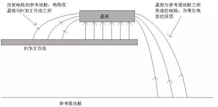
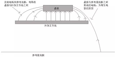
It can be seen from the figure that when the crystal oscillator is arranged in the middle of the PCB, or far from the edge of the PCB, due to the existence of the working ground (GND) plane in the PCB, most of the electric field is controlled between the crystal oscillator and the working ground, that is, in Inside the PCB, the electric field distributed to the reference ground plane is greatly reduced, resulting in reduced radiated emissions.
3. Handling measures
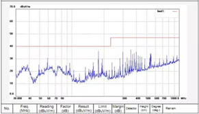
Move the crystal oscillator inward so that it is at least 1cm away from the edge of the PCB, and apply copper on the surface of the PCB within 1cm of the crystal oscillator, and connect the copper on the surface layer to the PCB ground plane through via holes. The spectrogram of the modified test result is as follows, it can be seen from the figure that the radiated emission has been significantly improved.
4. Thinking and Enlightenment
Capacitive coupling between high-speed printed lines or devices and the reference ground plane will cause EMI problems, and sensitive printed lines or devices placed on the edge of the PCB will cause immunity problems. If the design must be arranged on the edge of the PCB due to other reasons, then a working ground wire can be placed on the edge of the printed line, and more vias are added to connect the working ground wire to the working ground plane.


